A digital VLSI controller for an automotive turn-signal system — four LED clusters of three LEDs each, sweeping 000 → 001 → 011 → 111 for the directional effect, with hazard and brake overrides. Built end-to-end on a custom 65 nm standard-cell library: transistor-level layout in Cadence Virtuoso, RTL synthesis in Design Compiler, P&R in Innovus, and signoff against zero DRC/LVS errors with +14.47 ns of timing slack at a 60 ns clock.
The chip drives four external LED clusters — Front-Left, Front-Right, Rear-Left, Rear-Right — each containing three LEDs that illuminate sequentially (000 → 001 → 011 → 111) to create the sweeping visual effect of a real turn signal. The behavior is governed by an FSM that arbitrates between the directional switches, hazards, and brake input according to standard automotive priority.
Because the system runs on a high-frequency internal clock, the design integrates a 45-bit ripple-carry adder used as a clock divider that scales the input clock down to a human-perceptible blink rate. This divider, not the FSM, ends up being the chip's critical path — and the central engineering decision of the project.
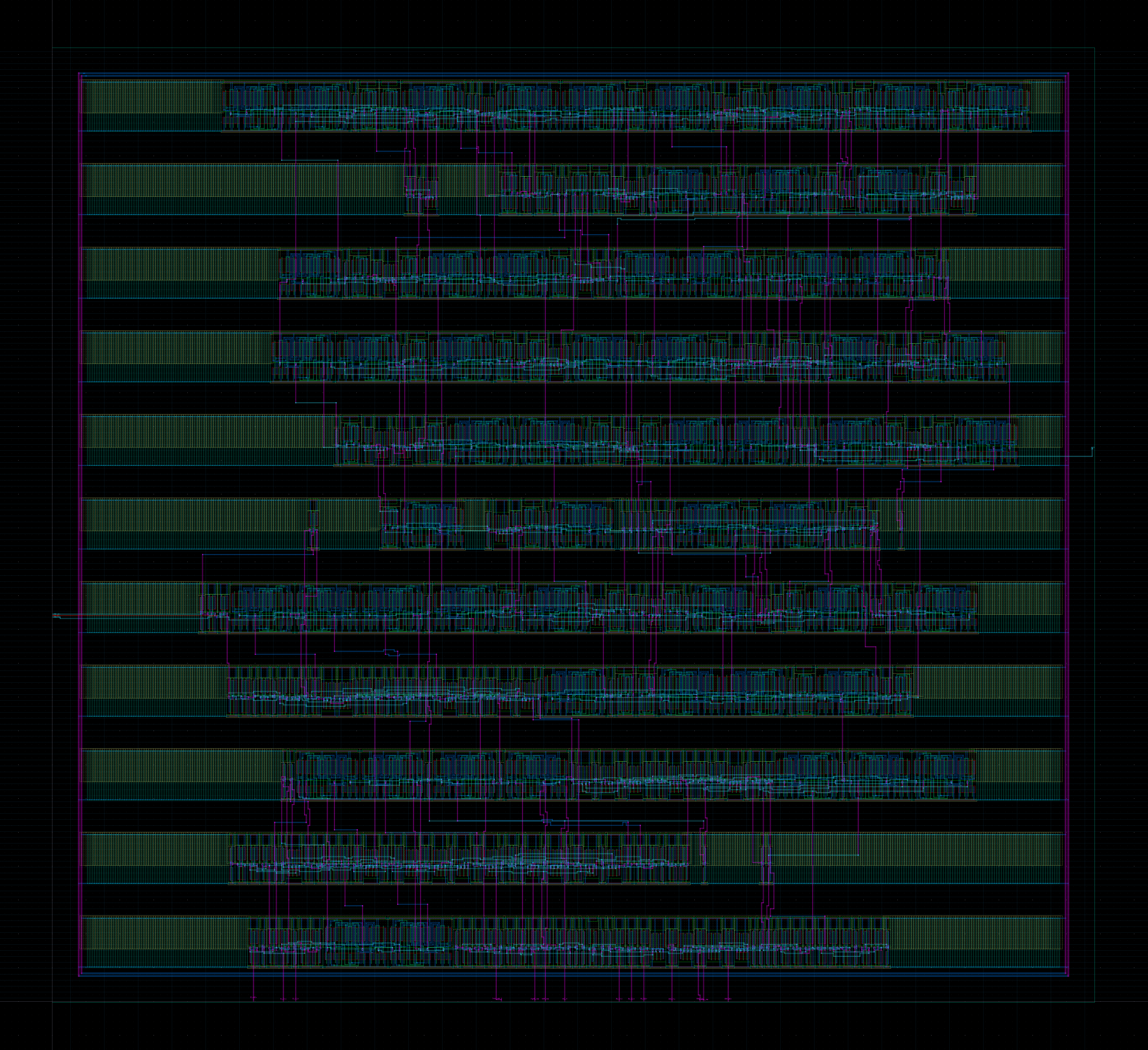
[ click to zoom · 7680×7022 ]
Designed and verified a complete custom standard-cell library targeting the GlobalFoundries 65 nm process. Every cell was hand-drawn — schematic, layout, and verification — instead of pulling from a vendor PDK. The library covered the gates needed to synthesize the rest of the chip:
I used stick diagrams to optimize Euler paths through each cell, minimizing diffusion breaks and the parasitic capacitance that comes with them. Layouts adhered to strict standard-cell methodology — fixed cell height, aligned VDD/GND rails, clean PR-boundary constraints — so the cells would tile cleanly during automated placement.
Every cell got its own Calibre DRC and LVS pass before being released to the library. After layout I ran parasitic extraction (PEX) and characterized each gate analog-domain in HSPICE to pin down intrinsic delays and drive strengths — the data the timing tools later relied on.
The turn-signal FSM and the 45-bit clock divider were written in Verilog RTL. Pre-synthesis functional verification ran in ModelSim against a testbench driving the clock and switch inputs through every transition — left, right, hazards-overriding-directional, brake-forcing-rear — to confirm the sweep generated the expected LED states.
From there, Synopsys Design Compiler mapped the RTL onto the custom gate library from Phase 1, producing a structural gate-level netlist. Because the synthesis target was my own library, any mistake in a cell would have shown up immediately as a timing or area regression — the cells got a second round of validation for free.
The clock divider was the single largest architectural decision of the project. To divide the system clock down to a human-visible blink rate, I needed a 45-bit counter — and the choice of adder topology directly trades chip area against critical-path delay.
A carry-lookahead or carry-save adder would have cut path delay dramatically but exploded the cell area and routing congestion needed to wire it up. An automotive blinker runs at human-visible frequencies — sub-Hz — so paying for adder speed I'd never use was the wrong tradeoff. I optimized for area and accepted the slower 45-bit ripple-carry structure.
The consequence: the 45-bit ripple logic becomes the chip's critical path. Final STA capped the maximum operable clock frequency at ~21.9 MHz — orders of magnitude above what the application actually needs, and the right call for the use case.
The post-synthesis netlist went into Innovus for the physical build. Generated the power rings and stripes, placed the custom cells into rows, and ran the automated metal routing — connecting all of the FSM and divider logic while staying clear of DRC violations.
| Feature | Measurement | Value (μm) |
|---|---|---|
| Width | Metal-to-Metal (M2) | 146.54 |
| Width | PR Boundary (total) | 154.18 |
| Height | Metal-to-Metal (M1) | 133.68 |
| Height | PR Boundary (total) | 141.12 |
Final verification ran in three tools: Calibre for physical sign-off (DRC, LVS, PEX), PrimeTime for static timing analysis and power estimation, and HSPICE for post-layout transistor-level circuit validation.
STA placed the critical path running from clk_div_reg[0] through the 45-bit ripple chain to clk_div_reg[44]. Data arrival time on this path is 44.73 ns; combined with the flip-flop setup time of 0.80 ns, the absolute minimum required clock period is 45.53 ns. I set the clock period to 60.00 ns to leave margin, which yielded a positive setup slack of +14.47 ns (MET).
Total dissipation came in at 0.0356 mW, with the clock network accounting for roughly 78.9% of that — exactly what you'd expect from a 45-bit divider toggling on every cycle.
A full 45-bit divider sweep is computationally prohibitive in an analog solver, so post-PEX HSPICE focused on connectivity and signal integrity rather than full functional simulation. Output nodes showed clean ~40 mV clock-feedthrough spikes precisely aligned to the system clock's rising edge — confirmation that the electromagnetic coupling visible in the routed silicon was being modeled correctly by the extracted parasitics.
Phase 1 — Pre-layout (digital). The Verilog was driven by a ModelSim testbench that exercised the clock and every switch input, confirming the FSM transitioned correctly through all the sweep patterns and respected the hazard / brake overrides.
Phase 2 — Post-layout (analog). After Calibre PEX, the extracted netlist — with thousands of parasitic Rs and Cs — went into HSPICE. The simulation validated layout connectivity and confirmed signal integrity through visible clock-feedthrough behavior on the outputs.
The thing I'll carry from this project is how often the right move in physical design is the boring one. The 45-bit ripple-carry adder is slower, simpler, and uglier than the carry-lookahead alternative — and it's the right answer because the application doesn't care about adder speed. Letting the use case dictate the tradeoff instead of defaulting to the “better” structure was the most useful instinct to build.
The other lesson was how much of sign-off is just bookkeeping discipline — clean cell names, consistent rail orientations, careful constraint files. By the time I got to PrimeTime, the things that closed cleanly closed because of decisions made weeks earlier in Virtuoso.